> EUV necessitates an entirely new way to generate light. It’s a remarkably complex process that involves hitting molten tin droplets in midflight with a powerful CO2 laser. The laser vaporizes the tin into a plasma, emitting a spectrum of photonic energy. From this spectrum, the EUV optics harvest the required 13.5-nm wavelength and direct it through a series of mirrors before it is reflected off a patterned mask to project that pattern onto the wafer
This is incredible and feels like the most sci-fi sentence I've read in a long time.
It's unbelievable to think that this works, not just in a lab, but in commercial systems that will produce hundreds of chip wafers an hour (>100 anyway, they didn't clarify further).
It's also terribly inefficient. EUV "mirrors" eat 30% of the incoming light. Since they have such a narrow reflective range and the source light isn't collimated or coherent, you have to use a bunch of them. By the time you're at the mask, you've lost 96% of the light. As a result:
>Hynix reported at the 2009 EUV Symposium that the wall plug efficiency was ~0.02% for EUV, i.e., to get 200-watts at intermediate focus for 100 wafers-per-hour, one would require 1-megawatt of input power
It's an damn good question of how much further this can scale. EUV photons are a lot more like x-rays than they are visible light. They're energetic enough now they're inflicting ionization effects on photoresist material, blurring the exposed area with secondary electron scatter. The fundamental limit of electronic transistors, ones made out of single molecules, are going to be tough to make with lithography.
Still, 1 MWh is a tiny fraction of the power those 100 wafers worth of chips will consume in their lifetime. So if we can reduce power consumption with smaller features, it's worth using more laser power.
That makes me wonder (as someone who has merely heard of the two technologies and knows nothing much about either beyond the Wikipedia page) why it's not using a free electron laser?
Aren't those tuneable to any wavelength down to X-rays?
> This form of maskless lithography has high resolution but low throughput, limiting its usage to photomask fabrication, low-volume production of semiconductor devices, and research and development. [1]
The beam has to scan across the entire wafer instead of exposing it all at once, so it's extremely slow and uneconomical for mass production.
I'm fairly sure they're two different things: e-beam (as per your link) does the reaction with the electrons themselves, whereas FEL uses an electron beam as a lasing medium.
It's worth noting that necessity has tendency to make this possible though: the original CD laser diodes required extreme equipment investment to mass produce.
You could conceive of making the speed up in parallel production.
IIRC you can't usefully do that, because the limit is from the combined electric field of the electrons in the beam(s) causing blurriness — more beams at fixed current per beam means more blur.
Treat it like a phased array, with hypermegamodulation by realtime machine learning artificial fuzzy logic, canceling out any blurriness in advance, producing the finest and sharpest turbonanoscalpels, able to etch any sketch, fast. Built to last!
Isn't that similar to synchrotron x-rays? I just watched a video where they say that that's what people started with before they went with the tin plasma method.
The final challenge will be cost: With every iteration, costs increase dramatically. At some point, it simply ceases to make sense to scale down transistors any further.
Cost has been the challenge for the past 30-40 years at least.
Many semiconductor manufacturers have folded, dropped out, or merged over the years due to costs putting development of the next node out of their reach. If the remaining 3 drop out of the race, they will be following the same pattern as many before.
R&D and tooling costs have grown enormously to bring new fab process nodes online, but the actual per-wafer costs of materials and operating expenses historically haven't been growing to the same alarming degree. But that's changing, as new nodes are increasingly relying on power-hungry tools with low throughput that wear out mask sets at an unprecedented rate. It's not implausible for the industry to reach a point where new leading-edge processes will never mature to the point that they make economic sense for the low-cost applications that currently stay a few nodes behind the leading edge.
The problem here would be that if mask sets wear out at an unprecedented rate, it might not make sense to use these cutting edge nodes in the future (if/when we're several nodes ahead by then) for the things that currently use older nodes. Maybe Moore's law is dead for the types of things that stay 2 or 3 nodes behind state of the art all the time.
That was because of competition. The cost per transistor actually went down by a lot. If it soon goes up significantly, it will stop to make economic sense to increase transistor density any further. Why pay the same amount of money for a less powerful chip?
Maybe it will make sense for mobile SoCs or some other energy constrained applications which benefit from lower power draw of smaller process node chips. But power efficiency can outweigh lower absolute performance only to some degree.
> That was because of competition. The cost per transistor actually went down by a lot.
I'm not talking about the marginal cost to make the device, I'm talking about the R&D and capital expenditure to develop and build the machines for the next node.
You can be reductive and say it always boils down to competition, but then you would also say that ultimately shrinking will end when it can no longer compete with mature nodes. Competition in both cases. So I'm not sure what exactly that's getting at.
> If it soon goes up significantly, it will stop to make economic sense to increase transistor density any further. Why pay the same amount of money for a less powerful chip?
That's not strictly true, performance of a transistor still has value. Companies like Apple pay premiums to get in early on leading edge nodes, more per device than the mature nodes they move from.
Competition with "mature nodes" is different in the sense that here one company (like TSMC) will be "competing" with itself. They will just stop building next gen fabs if their chips wouldn't sell.
> That's not strictly true, performance of a transistor still has value. Companies like Apple pay premiums to get in early on leading edge nodes, more per device than the mature nodes they move from.
Apple can't increase the price of their product arbitrarily. So if the price per performance increases, the new iPhone would be slower than the old one. Maybe people will still buy it if it has better power efficiency, but that is a trade-off which has its limits.
> Apple can't increase the price of their product arbitrarily.
Not arbitrarily, but IIRC Apple's profit margin on iPhones is over 100% - the iPhone 14 Pro max is supposed to have a BoM cost of ~470 $ and retails for well over 1000$. That means Apple can both afford the high upfront premium/R&D cost of going to a smaller node and to eat up higher SoC costs and yet still have a profit per unit that would lead most other companies' CFOs to drool.
On top of that, even if the economics should not work out for mobile... a fully spec'd out M2 Ultra Mac Pro runs at ~14.000$, Intel ones IIRC could reach 50.000$. The crowd that pays such absurd prices has zero problems paying a grand or two more for higher performance.
> Competition with "mature nodes" is different in the sense that here one company (like TSMC) will be "competing" with itself.
No, why? Lots of foundries out there that don't compete on leading edge nodes.
> Apple can't increase the price of their product arbitrarily. So if the price per performance increases, the new iPhone would be slower than the old one. Maybe people will still buy it if it has better power efficiency, but that is a trade-off which has its limits.
That doesn't address what I said -- that price per transistor is not the single limiting factor. I never said any performance increase is worth infinite value.
The discussion moved to talking about is competing with mature nodes, where you said they'd only be competing with themselves (which doesn't seem to be right).
No, the point was that the leading edge will stop advancing when it can no longer compete economically with companies that sell mature nodes. Which is obvious, but I was just being similarly reductive.
> The point is that they will stop scaling chips before technical limits are reached.
Sure, like most commercial ventures, cost becomes prohibitive at some point and overtakes benefits. As it always has been.
> No, the point was that the leading edge will stop advancing when it can no longer compete economically with companies that sell mature nodes.
The "mature node" here will just be the one before the first node that doesn't make economic sense anymore. And this will be from a leading edge company, most likely TSMC. Say, if 2nm is too expensive compared to 3nm, then TSMC will stick with 3nm.
But when it comes to cost, evidently replacing many passes and other complicated processes with DUV machines with fewer EUV passes is a net win. And the energy required to create these chips must be a small fraction of the energy they will use in their lifetimes, so improved efficiency of the smaller nodes enabled by EUV would surely be a win, all else being equal.
I wonder what the possibilities for a fundamentally different manufacture method are. For example, what if we could program a layout into DNA and have biological agents construct it?
Well, unless one devises a way to break up atoms + rearrange those in such a way as to turn protons, neutrons, quarks etc. into compute machinery, we're stuck with individual atoms (or small groups of those) as the smallest possible building blocks. And thus Moore's law will hit a brick wall at some point. 3D structures (stacks w/ many layers of transistors & interconnect) will help, but make thermal issues more difficult than they already are.
Kind of like (iirc) the tip of a scanning tunneling microscope might be used to pick up & manipulate individual atoms.
Self-organizing materials like DNA might make that process easier, not scale it down further.
Once "gently" to deform it briefly into a concave shape, and the second, harder pulse to actually activate the droplet to emit extreme ultraviolet light
Anyone who reads these descriptions and doesn’t realize this is literally the magic of sorcerers predicted in our fantasy lore have lost the ability to dream. What an amazing time to be alive.
I'm quite sure they know the difference between real engineering and pretend engineering and I can guarantee you there is no duct tape in there, each and every last residual effect is part of the model, if it weren't it wouldn't work at all. The scales you're talking about imply that even the tiniest parasitic effect that you could safely ignore otherwise is going to utterly dominate your work if you don't account for it.
And yet that duct-taped machine can consistently fire two laser beams at a single droplet of molten tin hundreds of times an hour. Pretty magic if you ask me.
Asianometry is an amazing channel for topic like this. Also check the video on water for chip manufacturing. You’d never think there so many interesting challenges with something so mundane as water.
Modern chip manufacturing is basically black magic.
It's a bit worse than "zero appreciation" in some cases, it's people using the results from hundreds of years of advances in science and engineering to proudly post their anti-scientific viewpoints.
i.e. there absolutely cannot be any obligation to subscribe to the ideology of either team eddison or team westinghouse in order to make use of a light switch.
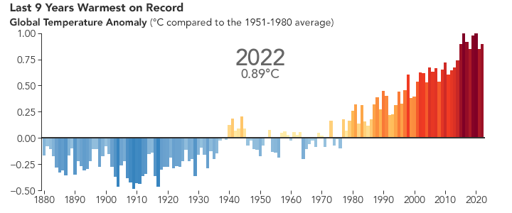
I'm sorry but CO2 being the primary driver of climate change was predicted in the 50s. Back then it was just a hypothesis and now it is undeniable.
Meanwhile the competition that was "bullied into submission" made ridiculous claims like global cooling all the way until 2014.
Inform yourself about a topic before talking about it.
Here is the ancient paper: [1]
If you check the prediction in the abstract it mentions doubling CO2 levels, which means going from 310ppm (1955) [2] to 417ppm today or a 33% increase. The paper predicts a 3.6°C increase and 33% of that is around 1.18°C which is dead on.
The temperature record goes back to 1880 but when you look at the relative warming then 1950 and 1880 had the same temperature [3] so it doesn't matter that IPCC numbers start from 1880 instead of 1950.
If you think predicting a single number and doing it this badly (temperatures), 33% within the correct value, and calling it science, you're the problem.
Oh and nice cherry picking. With the given variable and its pretty small variance, I can cherry pick models too, and claim it is the rain god's judgement, or whatever.
The fact that IPCC's models currently barely even give a consistent prediction, and the variance between them is so high, shows this isn't science.
Everyone's attributing the signal in the models to CO2 or climate change, while the most reasonable explanation, is that the signal is a result of the agreed upon biases and approximations that everyone in "climate science" is copying from each other, and it is also clear that models that were developed independently give more diverging results, the Russian model even predicting cooling.
HN will also happily exclude companies like ASML from their definition of a "tech" company, because most of their value doesn't come from their software IP.
> And that is sad part of so called "Tech" today. Zero appreciation of it outside of the minorities.
This has always been true of technology.
Do you think most people cared about how a steam engine worked, or simply that it allowed them to go faster than a horse? Or the telegraph, radio, television, the internal combustion engine, etc.
Even more crazy that process runs at 50khz, that is vaporizing 50,000 droplets per second. This is necessary because the overall efficiency is really poor vs the energy density they need on the chip to react with resist.
I worked at Imec back in 2005 alongside the teams installing and researching the first EUV machines from ASML. Never thought they’d get it to work given the technological challenges. Laser-pulsed tin plasma, mirrors instead of lenses and vacuum exposure just to name a few!
Glad they got it working so we can print smaller at scale.
Friend of mine worked for an asml supplier. He was working on adjusting the optical path based on how the laser going through a lens heats that lens up and changes its optical qualities. There are so many challenges we don't even think about
Building a modern semiconductor factory starts long before you can begin to think about the foundation. Minimizing vibration is included in thinking about the siting, seismic insulation of the building and the placement of just about everything in the fab itself.
Think 'boxes in boxes' to get maximum insulation. I also have a friend who works in this industry and he once joked that they have an almanac built in to deal with moon tides and while it is a funny joke you have to wonder if there isn't going to be a time when even that sort of effect will have to be accounted for. Amazing stuff.
ASML is one of a short list of Dutch companies that I'm super proud of, they keep on innovating no matter how extreme the challenges are. The moat they have is incredibly deep.
When you go to the extremes those tiny details suddenly aren't tiny details anymore. As a semi-random example, a significant source of noise in LIGO, the gravitational wave detectors, is the push of photons striking the 40kg mirrors[1][2].
There were years of hope in the semiconductor industry that somebody would come up with something better rather than having to make that nightmare work.
Alternatives were tried. Synchrotron EUV sources. (works, but huge).
Linear accelerators (The SLAC beamline was used as a light source as a test). X-ray lasers (don't work yet). Electron beam lithography (works, but too slow.)
Whatever happened to Multibeam? [1] They claim to sell a multiple electron beam writer for maskless chip making. They, and their predecessor company, have been at this since 1980. Not much new on the web site, and their last press release was in 2020.
I recently had an opportunity to chat with a machinist who works for a shop that makes some parts for ASML’s machines. He showed me a picture of a couple of parts he finished that day. He said they weighed about a hundred pounds sitting there on the table, but at the acceleration they experience in the machine, they weigh roughy the same as a Toyota Tacoma.
I can't imagine that what I think of as a machinist - a human who picks up parts and places them into machine tools and adjusts settings - is who makes parts for semiconductor manufacturing machines. I'm guessing the title has a lot more to do with CNC/automation these days?
FWIW the Bridgeport milling machines could hit 1/10,000th of an inch which is 25 microns of accuracy many years ago. DRO and precisely controlled steppers on newer machines can do much better.
The main difference is the mill will be that accurate along each axis of motion independently, while the jig borer will hold that accuracy on all 6 degrees of freedom throughout the full workspace volume.
You kind of just described the job description of a modern "machinist". It's far more of a job regarding the machine itself (CNC in this case) and it's setup, versus the part itself being made. A mechanical engineer or manufacturing engineer deals moreso with that. Machinist is more synonymous with "operator" in my field.
The industry's currently shipping chips based on the 3nm process. I understand that it's mostly a marketing term (i.e. non-standardized), but I assume the actual transistor channel is within that order of magnitude.
Knowing that a silicon atom is larger than 0.1 nm, how can we possibly keep Moore's Law on track? It feels like we're close to hitting fundamental limits.
We are ridiculously far from physical limits in our current artificial computers (both theoretical [1], and practical [2]). For more technical details see Jim Keller: [3] [4] [5].
[2] The ~12 watts computer inside each living human adult skull (and perhaps each eukaryote cell [6]) is still the state-of-the-art, for quite some time.
[6] Our computers aren't yet able of polycomputation, where the computation topology, data, and functions depend on the observer, instead of computation in a passive implementation, once done forever set in s̶t̶o̶n̶e̶ silicon, 2023, Michael Levin, Agency, Attractors, & Observer-Dependent Computation in Biology & Beyond, https://www.youtube.com/watch?v=whZRH7IGAq0
Physical limits don't matter much when economic limits (transistor cost) are reached much earlier. What matters is not transistors per chip area (Moore's law) but FLOP/s per chip cost. Also FLOP per chip power draw.
Economic limits are imaginary, secondhand effects of the ideological goggles one's society decides to wear at a certain time for arbitrary reasons. USA during the Manhattan Project knew of no economic limits, i.e. they could arbitrarily push them according to the greater goal; China today, for instance, knows no economic limits. But yes, today, in the "Western" world a speech such as "we choose to get 160 zetaflops (10^21) [1] under your desk in 10 years because it is hard" [2] would be unimaginable, also because you can count on the fingers of an amputated arm how many politicians know what a FLOP is.
Interestingly enough, penny pushing also destroys capitalism, see The Man Who Broke Capitalism: How Jack Welch Gutted the Heartland and Crushed the Soul of Corporate America―and How to Undo His Legacy [1].
Sure, we are close to the end of silicon semiconductor improvements. And Moores law could be near its end. In fact the price per transistor has not been dropping recently, so it may be over already.
If there’s hope for the future, it’s that there are many other computing technologies besides traditional silicon that show potential, so maybe the torch will be passed to quantum, or superconductors or dna or something else.
Peak applications require the latest and most powerful tech. With it’s colossal trail of pollution from manufacturing.
For the rest I often wonder if would not be better for the environment to re-purpose older, already made tech.
Plenty of embedded systems grinding on for a long time.
And user facing applications lack one thing: public stats of peak system usage. When confronted with a new purchase we should be handed over a sheet of our own and peers statistics. Producers and service providers have them anyway.
In an ideal world, the cost of everything we buy would include the real costs of pollution (including greenhouse gases), depletion of common resources such as water, and recycling or otherwise accounting for the environmental impact after use.
As you say, suddenly those 5 year old phones and computers would be economically attractive again. With a knock-on effect that websites and software would cater more for older devices.
Note that I'm not at all saying that we shouldn't have companies like ASML researching processes like this - more efficient chips are good for the environment and the economy.
Try & view compute power as order of magnitude, vs. what useful things can be done with it.
Something containing ~100k transistors, ~10KB RAM & flash, running at a few MHz in a power envelope measured in milliWatts, has production cost (and environmental footprint) of practically 0 these days. But still enough brains to control your washing machine, monitor solar panel or open garage door w/ remote.
A few steps up & you have epaper equipped tablet that allows you to read books, simple games or check weather forecast, doing so for days or weeks on battery power.
On the other end of the scale you have datacenters, supercomputers & their energy + manufacturing footprint. With desktop PC's, laptops & game consoles somewhere in between.
When choosing between:
a) Apply budget, see how much CPU, GPU, RAM etc. that buys you, and deal with physical size + power draw / thermals, these days I go for
b) Pick physical size + power budget, see what kind of CPU / GPU / RAM etc you can shoehorn in there @ what cost, and just deal with the limitations of such device (if perceived as limiting, that is).
It's amazing what a Raspberry Pi sized computer (or further down, a modern uC) can do these days. Lean software does exist. No clunky desktop needed if you just want to play PacMan. :-)
How does 13.5nm light etch features of 7nm and lower? I can sort of see how ultra pure water can focus the light (immersion lithography) and multi patterning (I’m not sure how this works really, I would have thought shining light through two masks would make things even more blurry). When the photon hits the silicon why isn’t the dot 13.5nm?
The one thing I can answer is that multi-patterning does not shine light through two masks simultaneously. Instead, it consists of multiple separate steps.
I think for the rest, the point is that light arriving on the waver is not a binary thing, but due to refraction and self-interference light arrives in variable intensities. So within difficult constraints, this allows you to control the area in which the intensity is below our above certain thresholds. I assume that if you then manage to control the chemistry just right, you can then produce features that are smaller than the wavelength of the light -- under severe constraints of what shapes you can produce. You definitely do not get to produce an arbitrary bitmap of sub-wavelength pixel size.
If you drag a baseball bat through sand, the edge of the cut "channel" is much sharper and narrower than the baseball bat.
Now offset the baseball bat a bit and draw another line which is partially overlapped over the first one. You will get the intersection of the two baseball bat wide channels, but it will be much narrower.
masks dont have the actual shape, but shapes accounting for wave interference patterns that will end up producing the final shape when EUV light passes through. I believe the process of comming up with the correct intereference pattern takes weeks of supercomputing.
I think I've listen to asianometry (YT channel) talk about this too, but I am unable to find any clip now where he explicitly talks about interference lithography...
I don't know, I've been working with LLMs a lot recently and for the first time in a while I am wishing I had access to much more compute than I do. Imagine having the power of a H100 locally without having to pay thousands of dollars a month.
For inference, at least locally, the bottleneck is usually the memory bandwidth (and quantity, of course).
I hope that AI hype lead us to more memory and more memory bandwidth, because they are really lagging behind computer power increase from like 15 years already.
Oh, 100%. But you can do some pretty amazing things with fine-tuning LLMs too, and that is very compute intensive. Not to mention it's ridiculously hard even getting access to a cloud GPU instance nowadays.
Get used to it. The memory wall is coming and if you are in the industry it's possible that within your career you may need to adapt to falling DRAM-to-core ratios.
The memory wall arrived decades ago. That's why caches were invented (which don't solve the problem, just soften the blow).
One approach would be to snip RAM in as many pieces as you have cores, and attach each piece locally to a CPU core. Say eg. 1k cores each with 1/1000th of total RAM, accessible at L1 cache like speeds. Giving you crazy-high (combined) memory bandwidth. I know, there exist some IC's that actually do this.
Problem is such a setup is not suitable for all types of computation. For data structures that require individual cores to access other cores' local RAM, you still need some communication protocol (+ latency, bringing you back to square 1).
And we haven't quite figured out how to program such a beast in software developer-friendly way.
Hence the usual approach of "all RAM in one pile, connected via a fat pipe to a heap of CPU cores".
I'm not sure what "standard computer configuration" means. Maybe you mean a budget laptop? Your typical new gaming desktop build is 32GB, and for a workstation probably 64GB.
I think you can get a 2TB ssd for like a 100 bucks nowadays. They are dirt cheap.
Gaming desktops are not even close to being a standard computer configuration and you know it.
I’m talking about the typical computer you’re going to find in a big box store or the default configuration on a website.
Yes you can add an SSD yourself for that price but the markup for configuring it at purchase is considerably more than $100. I’m not talking just Apple when it comes to this, Dell, Lenovo, HP, Microsoft, and just about everyone else do it too. RAM is even worse now that many (most?) laptops have it soldered in, so there is no DIY upgrade after you buy.
> RAM is even worse now that many (most?) laptops have it soldered in, so there is no DIY upgrade after you buy.
From the cursory look to an e-shop, it seems to me that majority of notebooks have soldered-in memory, but also one SIDIMM slot for expansion. Just the very low-end ones (and Apple) have no SODIMM slot.
And 16 GB is definitely the most populous category of notebooks.
Sorry I don't follow how this "standard" configuration is relevant. If you want more just buy more? If you don't want to pay pre-built markups build it yourself.
And the point about gaming setups is very relevant because you can get consumer hardware (aka cheap), instead of being forced into "workstation/server" which carries a huge markup.
You can get 128GB RAM and stupid amounts of ssd storage for cheap with consumer hardware.
The hardware hasn't stagnated at all. I think you're problem is simply with pre-built markups?
As a developer I care because that’s what my users have. As an employee I care because that’s what my employer buys for me to use at work. As the unofficial IT support person for my friends and family I care because that’s what most of them will buy and ultimately ask me to help with.
Also if you want a laptop, the markups for upgrading said memory and storage are actually pretty significant and may not be worthwhile. Upgrading laptops is quickly becoming difficult to impossible. Yes I know about Framework, but they are not ever going to be mainstream for a number of reasons.
thou, 8gigs are overly common (and overrepresented in regard to your market analysis) as most consumers (and enterprises) tend to buy the low-end config unless it's absolutely necessary to spend more.
The problem is the difference in pricing between the 16 and the 32gigb one, the manufacturers are taking advantage of the sodering which is almost going to be the default in the upcoming days, and taking consumers for a ride.
Von Neuman's architecture has run out of steam. The fact that most transistors in a computer at any given moment are idle seems to be a huge waste. What if you could just have a computational fabric that lets you have one instruction per cell, and run whole programs in parallel?
FPGAs do that, but the "smart" routing fabric in them makes compiling code to them take hours or days.
If you eliminate the switching fabric on an FPGA, you are left with a grid of Look Up Tables (LUTS) each connected to their neighbors. The result is a Turing Complete computer that works exclusively in parallel.
At home (which is also my workplace) all my PCs are at 128GB. The server is 512GB. Laptops are 64GB. RAM has not been stagnated. Just buy what you need. To get it cheap for example for laptops I would buy smallest configuration (RAM and SSD wise) but with good CPU. I would then throw out old RAM and SSD and replace with the ones I buy separately. Way cheaper this way. PCs and servers are assembled from parts. Again I just order what I need and then let custom PC maker nearby assemble it for me.
For general office computing or media consumption, yes, the 'standard' is indeed laptops, tablets, phones, consoles and TV's.
For locally playing with AI, those are a joke. A beefy desktop gpu, preferably with 24GB vram, a nice desktop high threaded cpu. 64GB of ram and as many TB of fast M.2 storage you can afford is the starting point.
Those OSS LLM models will eat your typical enthusiast gaming PC for breakfast.
Depends on your demographic, I guess. My 8-year-old desktop was built with 16GB and that was middle of the road even then. Only a 64GB SSD at the start, though. I didn't see laptops really take over from desktops for a few years after that.
Your story doesn't really add up. 8 years ago would have been 2015, at which point 64GB drives had been dropped from most consumer SSD product lines for at least a year, and laptop sales had been outnumbering desktop sales by a wide margin for many years. I don't think you realize how thoroughly unrepresentative your experiences and purchasing choices have been.
This has gotta be peak HN. "I built a desktop 8 years ago using these components which were pretty normal at the time." "No they weren't." There were like 10 different brands of 64GB 2.5" SATA SSDs to choose from at the time, in the most popular PC components shop in the city, so it wasn't just my little niche. Plenty of people had laptops, sure, but most daily-driver work machines were still desktops.
The minute you said custom built from components you went off the rails of my argument. There is nothing standard or common about that. Very few people build their own computers from components, nor should they. It also ignores the fact that most people buy laptops.
I am talking about the memory and storage configuration of the "typical" computer that an average consumer will buy from a big box store or a website. This has been 8GB/256GB SSD for a long time now. That is my source of complaint. Growing up in the 80s and 90s there would be absolute leaps in memory and storage every time you would upgrade your computer. That is no longer the case. We are just now starting to see some 16GB/512GB configurations appear on consumer default configurations after what, almost a decade?
> There were like 10 different brands of 64GB 2.5" SATA SSDs to choose from at the time, in the most popular PC components shop in the city, so it wasn't just my little niche.
Your story gets even weirder! Sourcing components from the local brick and mortar store when building your own desktop usually negates most of the benefits of building your own desktop computer. It's not entirely surprising that they had an excess of outdated SSDs on display.
> Plenty of people had laptops, sure, but most daily-driver work machines were still desktops.
Are we suddenly confining the discussion to corporate-owned office PCs, or do you genuinely not understand that laptops have been outselling desktops for a very long time?
Is this the one that Intel is getting first dibs on for the next few generations? Looks like these fabrication paradigms generally work on Moore's law for some time before tapering off (S curve to some degree) but the discovery of a new paradigm can slow down the overall trendline if it takes too long to commercialize.
Not going to happen. Remember, TSMC manufactures chips for Apple, Nvidia, AMD, Google, and a looot of other companies. They own about 60% of the cutting-edge fab capacity in the world, while Intel was basically an "also ran" during the transition to EUV.
ASML is never going to tie themselves to a single customer like that, let alone one which isn't even the market leader. High-NA is a massive technological change, and all the major players have already ordered their machines. Intel was simply the first to complete their order in a desperate attempt to avoid a repeat of their EUV debacle, but they'll receive their new toy at most a month or two earlier than their competition.
First dibs is not exclusivity, they simply were the first to order it and will be the first to receive the initial machines giving them a calendar advantage.
I assume these will be made available to Intel Fab customers as well at internally to Intel, since they are opening up 3rd party fabrication at a service offering.
ASML currently has a market cap larger than Intel. That has nothing to do with their sales but puts into perspective how important this technology is relative to all of Intel's activities. TSMC has been reported as their biggest client (https://www.reuters.com/technology/asml-shares-fall-7-after-...)
Intel is getting the first prototype(s), in a few years from now. Then add a a year or two before those EXE’s are actually used for volume manufacturing.
No exclusivity, as it’s ASML business model to work fairly with all semiconductor manufacturers.
They have the prototypes now, and are talking about entering mass production 2H 2024 [1]. From what I read, Intel has already received and taped out 18A and 20A using these new high-NA machines [2]
>Intel has announced that manufacturing of 18A-node chips will commence in H2 2024, six months ahead of schedule. According to a roadmap released last year, this node will be Intel’s first to employ high-NA lithography. It’s not clear whether this means that the next-gen EUV technology makes its debut in production a little earlier than expected. Last January, ASML CEO Peter Wennink told investors that he expected high-volume high-NA manufacturing to start in 2025 or 2026.
ASML high NA
Credit: ASML
ASML’s first high-NA system, the Twinscan EXE:5000, is fully production-capable, but chip manufacturers will initially use it for process development. The first unit will ship in H1 2023, with Intel on the receiving end. The US processor maker also placed the first order for the EXE:5000’s successor, the EXE:5200. The swift adoption of high-NA is an important element in Intel’s strategy to regain “unquestioned leadership” in the semiconductor industry by 2025.
Is there any indication that it’s possible to build subatomic size transistors? Last I checked the data, transistors are already only a few atoms in size (silicon and carbon atoms are somewhere in the 0.3nm range), and it was a widely held opinion that it would stop at that if not much sooner. That would keep Moore’s law alive for a bit longer at best but the end does seem in sight.
Even considering all of that the economics seem to have already stagnated in cost for performance.[1]
Bear in mind, when silicon foundries say they have an Xnm process, nothing in that process is actually Xnm. TSMCs 2nm process does not make transistors 2nm wide[1]. They are in fact, approximately 40-50nm wide. The process number is a marketing number, and what changes each generation is actually transistor geometry (here you'll see terms like FinFET and GAA transistor and such, plus some process improvements that cause "half" generations)
But yeah, the fact that latest process nodes actually increase in cost is why people say "Moore's law is dead". Performance improves, but to keep the trendline roughly exponential, many things have had to give since the late 2000s. Such as: cost per wafer, power usage for max performance etc.
One layman question here maybe someone with better knowledge of the field can answer: could it make sense at some point to work without masks and lights and have only large scale laser arrays that write the structures directly but in the smallest possible scale (electrons)? Wouldn’t such an array be more energy efficient, be able to acquire smaller scales and trough the parallel process at some point be as fast as current systems using masks + light?
This is called electron beam writing, and is done routinely in research settings and to write the lithography masks, but does usually not have the required throughput for a production line. The upside of mask-based lithography is that all structures are exposed at once.
A single beam column with the machine around it costs millions already, and takes quite some space. Wafers are simply not large enough to accommodate more than, I'd guess, two or three columns at the same time. Each with independent optics.
A somewhat simple 2x2 cm Si photonics Chip in my line of work takes about 24h exposure for two layers - a full scale wafer is hundreds of times larger, more complex, and has dozens of layers. The math, physics, and geometry just don't really work out (yet)
You would think you can make the lithography faster with electron beams by just having many beams in parallel. But as far as I understand that’s doesn’t really work if you try to have too many beams: keep in mind that the electron beams would be extremely negatively charged. So they’ll repell each other if they get too close.
Why aren't we going electron lithography? As a laymen I think it should easily be able to surpass EUV in terms of resolution. I would imagine there are very good reasons why we aren't seeing it.
Because it has absolutely awful throughput. Electron-beam lithography has an output measured in days per wafer. Meanwhile, EUV can easily output 150+ wafers per hour.
When the choice was made to go for EUV, E-Beam was actually the most mature technology available for next-gen lithography - but it just wasn't economically viable. The technology has remained in development over the years, but not a lot has changed yet.
It would have to be on the order of 1,000-10,000x cheaper for it be worth it. Not to mention that each wafer needs dozens of layers to function. So you will need to wait a very long time for all the layers to be completed.
Electrons are electrically charged, so a beam of electrons will interfere with itself. The only way around this is to have a very narrow beam, but that kills throughput.
It does highlight some potential pitfalls. Chiefly the rapid decay of muons and dealing decay particles. Also you need a source of high energy protons.
What surprised me the most is how little telemetry they have, almost none of it in real time. I guess the industry is used to just eating up the cost defects but it was mind blowing (or eye opening) to me.
This is incredible and feels like the most sci-fi sentence I've read in a long time.
It's unbelievable to think that this works, not just in a lab, but in commercial systems that will produce hundreds of chip wafers an hour (>100 anyway, they didn't clarify further).