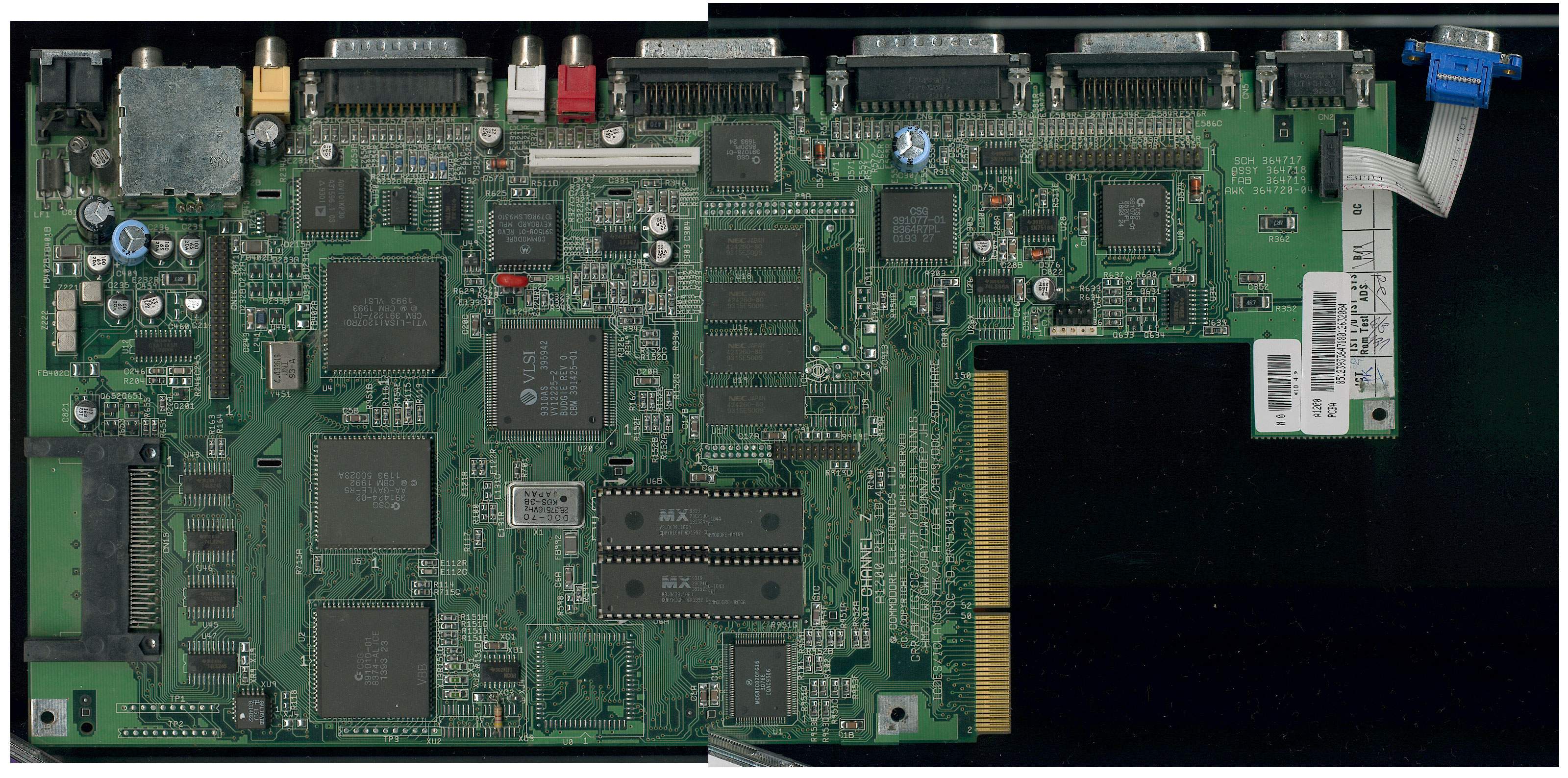
I'd be fascinated to have a breakdown of what all the ICs are on the motherboard. Like are they mostly ASICs, or mostly discrete logic, like level shifters, gate drivers, shift registers and the like?
Either way, it's amazing to think that basically every non-power related chip on that board is now inside a modern chipset IC.
Most of it is somewhat more high-level than the 7400-series ICs and such you might find in something older like the early 6502-based microcomputer motherboards.
Not sure about the rest, but I thought it was funny that the 80286 CPU is among the smallest chips on the board - that's probably due to the PLCC (?) packaging, while most of the others are DIP, but still...
The only other PLCC-packaged chips are two ATF1508AS, which are indeed ASICs (CPLDs) - oh, and the 53C400, which is... a SCSI controller (probably added as a bonus?!).
>I thought it was funny that the 80286 CPU is among the smallest chips on the board - that's probably due to the PLCC (?) packaging, while most of the others are DIP
That's basically it. The 286 has a much larger wafer inside than a typical DIP, and DIPs are extremely inefficient packages.
It would be interesting to see how much you could shrink this board down if all these chips were replaced with BGAs (using the same wafers inside). Obviously, that's not really feasible (no one is selling a BGA version of an 8259 interrupt controller, much less an 80286), but it would be interesting to see the dramatic size reduction, just from packaging waste. Also interesting would be if you designed a board using BGA versions of all these chips, but fabbed on modern IC processes (thus yielding much smaller wafers. and therefore somewhat smaller BGA packages). Of course, the whole thing could probably just be implemented with a single FPGA these days.
Either way, it's amazing to think that basically every non-power related chip on that board is now inside a modern chipset IC.